
This is an introductory article on how to program digital electronics in Verilog and simulate the result in Modelsim.
Verilog is a hardware language it is different from conventional High level language like C/C++. You need to think in a hardware style like how hardware works ? how these digital gates work ?
This tutorial will help you in understanding basics of Verilog and will present some examples on how you can simulate your digital circuit on Modelsim using Verilog.
See Tutorial on Modelsim here
Introduction: Verilog is Hardware descriptive language (HDL) and is standardized as IEEE 1364. The code you write in Verilog is translated to On-Off switches like machine language and can be transferred to FPGA (Field programmable gate array) which is a complex structure of digital gates.
Now before jumping ahead to FPGA’s we need to learn some basics of Verilog and make sure our code is synthesizable i.e. it must meet our hardware resources and is in working condition.
Verilog can be programmed in three main styles:
- Gate Level Modeling
- Data flow Modeling
- Behavioral Modeling
In “Gate Level Modeling” we design circuits like we do on breadboard and program the circuit by using gate names “AND”, “OR”, “NOT” etc. This is preferable for small circuits
In “Data flow Modeling” we use registers and assign statements to program the circuit. We design circuits in blocks and flow the data from on block to another. This is preferably for small to medium level circuits
“Behavioral Modeling” is the highest abstraction level of designing. It is very close to C/C++ language and make use of loops, switch statements and if-else condition. This sort of programming is needed if our design becomes too much complex to design its digital circuit.
Module: A module is a basic building block of a digital circuit. Think of it like a programmable IC you just input something and you get some output as shown below:
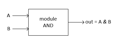
In the above figure inputs are “A” and “B” and the module is just doing the operation “AND”. Following rules must be remembered for designing modules:
- It must be ended with “endmodule”
- It must have a name, port list (defines inputs and outputs)
- It must have some functionality (like AND, OR etc)
- Modules cannot be nested
Module doing AND operation in the figure has the following code:
module andgate(a,b,out);
input a,b;
output out;
and gate_1(out,a,b);
endmodule
In the above code inputs “a” and “b” are passed through operation “AND” and the result goes to output “out”. Notice in the above code we have used a name “gate_1” after and operation on line 4. This is convention of Verilog and we must name each gate otherwise compiler will through error. Also following the rules of module we must have to name the module as well and here we named it “andgate” followed by the list of ports i.e. inputs and outputs.
Now we have created our first module which is doing a simple “AND” operation. Next what we need is a stimulus or Testbench which will be used to verify our design. Testbench will tell us if there are any errors in our code or if it is synthesizable or not.
To test our code we need a simulator like Modelsim or Xininx etc. We will discuss both in our future discussions. In the beginning we will start with Modelsim and will move towards Xilinx for implementing our design on FPGA. If you are using Modelsim then you need to create a testbench your self but if you are Xilinx it will automatically create a Testbench.
Testbench code for Module “andgate”
`timescale 1ns/1ns
module andgate_tb;
wire out;
reg a,b;
andgate mygate(.a(a), .b(b), .out(out));
initial
begin
a = 1'b1;
b = 1'b1;
#5
a = 1'b0;
b = 1'b1;
end
endmodule
Initially this testbench code looks vague but the main focus should not be this code at the moment. By the time passes this code will become clearer and you will get the hang of it on how these things works in real life. In the below figure we have simulated our code using Modelsim.
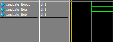
In the above simulated result we can see that for 0-5ns the output is 1 because both ‘a’ and ‘b’ are 1 where as in from 5 to 10ns the output is 0 because ‘a=0’ and ‘b=1’. Hence, our “AND” gate works as it should be. We can try for other input combination as well by just changing our testbench code.
More examples of gate level modelling using Verilog are discussed in the section: “Verilog Gate level Modelling examples“. Also see How to use Modelsim Tutorial.