
Following examples will help you a clear out understanding of Gate Level Modelling of Verilog.
Example-1: Simulate four input OR gate
Verilog code:
module orgate(out, a, b, c, d);
input a, b, c, d;
wire x, y;
output out;
or or1(x, a, b);
or or2(y, c, d);
or orfinal(out, x, y);
endmodule
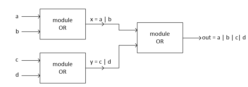
In the above Verilog code, we have used wire concept. Wires are used to connect modules just like on the breadboard. An output of one module is an input to another module and this can be performed by using wire. Wire ‘x’ and wire ‘y’ is the input to third OR gate as shown in the diagram below:
The key idea in Verilog or any hardware designing is to think in blocks and to write a separate code for each block. This idea will become clearer once we get the hang of Hierarchical style coding.
Testbench Code:
`timescale 1ns / 1ns
module orgate_tb;
wire t_out;
reg t_a, t_b, t_c, t_d;
orgate my_gate(.a(t_a), .b(t_b), .c(t_c), .d(t_d), .out(t_out));
initial
begin
// 1
t_a = 1'b0;
t_b = 1'b0;
t_c = 1'b0;
t_d = 1'b0;
#5 //2
t_a = 1'b0;
t_b = 1'b0;
t_c = 1'b0;
t_d = 1'b1;
#5 //3
t_a = 1'b0;
t_b = 1'b0;
t_c = 1'b1;
t_d = 1'b0;
#5 //4
t_a = 1'b0;
t_b = 1'b0;
t_c = 1'b1;
t_d = 1'b1;
#5 //5
t_a = 1'b0;
t_b = 1'b1;
t_c = 1'b0;
t_d = 1'b0;
#5 //6
t_a = 1'b0;
t_b = 1'b1;
t_c = 1'b0;
t_d = 1'b1;
#5 //7
t_a = 1'b0;
t_b = 1'b1;
t_c = 1'b1;
t_d = 1'b0;
#5 //8
t_a = 1'b0;
t_b = 1'b1;
t_c = 1'b1;
t_d = 1'b1;
#5 //9
t_a = 1'b1;
t_b = 1'b0;
t_c = 1'b0;
t_d = 1'b0;
#5 //10
t_a = 1'b1;
t_b = 1'b0;
t_c = 1'b0;
t_d = 1'b1;
#5 //11
t_a = 1'b1;
t_b = 1'b0;
t_c = 1'b1;
t_d = 1'b0;
#5 //12
t_a = 1'b1;
t_b = 1'b0;
t_c = 1'b1;
t_d = 1'b1;
#5 //13
t_a = 1'b1;
t_b = 1'b1;
t_c = 1'b0;
t_d = 1'b0;
#5 //14
t_a = 1'b1;
t_b = 1'b1;
t_c = 1'b0;
t_d = 1'b1;
#5 //15
t_a = 1'b1;
t_b = 1'b1;
t_c = 1'b1;
t_d = 1'b0;
#5 //16
t_a = 1'b1;
t_b = 1'b1;
t_c = 1'b1;
t_d = 1'b1;
end
endmodule
After simulating the code using Modelsim we get the following waveform:
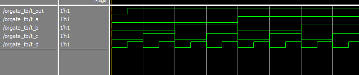
By observing the above waveform we can clearly observe that if all inputs ‘a,b,c,d’ goes to 0 the output is 0 otherwise it will be high as one of the input remains high which is the correct working of OR gate.
Example-2: Simultate the design given below:
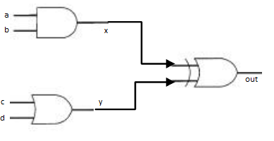
In the problem given above we can clearly see that inputs ‘a,b’ are ‘ANDed’ and ‘x’ is the output and input ‘c,d’ are ‘OR’ together with the result in ‘y’. Lastly, ‘x’ and ‘y’ are passed through ‘XOR’ gate with final output in ‘out’.
Verilog code:
module example_2_bl(out, a, b, c, d);
input a, b, c, d;
output out;
wire x, y;
and gate_1(x, a, b);
or gate_2(y, c, d);
xor gate_3(out, x, y);
endmodule
Testbench code is shown below:
`timescale 1ns / 1ns
module example_2_bl_tb;
wire t_out;
reg t_a, t_b, t_c, t_d;
example_2_bl my_bravelearn(.a(t_a), .b(t_b), .c(t_c), .d(t_d), .out(t_out));
initial
begin
// 1
t_a = 1'b0;
t_b = 1'b0;
t_c = 1'b0;
t_d = 1'b0;
#5 //2
t_a = 1'b0;
t_b = 1'b0;
t_c = 1'b0;
t_d = 1'b1;
#5 //3
t_a = 1'b0;
t_b = 1'b0;
t_c = 1'b1;
t_d = 1'b0;
#5 //4
t_a = 1'b0;
t_b = 1'b0;
t_c = 1'b1;
t_d = 1'b1;
#5 //5
t_a = 1'b0;
t_b = 1'b1;
t_c = 1'b0;
t_d = 1'b0;
#5 //6
t_a = 1'b0;
t_b = 1'b1;
t_c = 1'b0;
t_d = 1'b1;
#5 //7
t_a = 1'b0;
t_b = 1'b1;
t_c = 1'b1;
t_d = 1'b0;
#5 //8
t_a = 1'b0;
t_b = 1'b1;
t_c = 1'b1;
t_d = 1'b1;
#5 //9
t_a = 1'b1;
t_b = 1'b0;
t_c = 1'b0;
t_d = 1'b0;
#5 //10
t_a = 1'b1;
t_b = 1'b0;
t_c = 1'b0;
t_d = 1'b1;
#5 //11
t_a = 1'b1;
t_b = 1'b0;
t_c = 1'b1;
t_d = 1'b0;
#5 //12
t_a = 1'b1;
t_b = 1'b0;
t_c = 1'b1;
t_d = 1'b1;
#5 //13
t_a = 1'b1;
t_b = 1'b1;
t_c = 1'b0;
t_d = 1'b0;
#5 //14
t_a = 1'b1;
t_b = 1'b1;
t_c = 1'b0;
t_d = 1'b1;
#5 //15
t_a = 1'b1;
t_b = 1'b1;
t_c = 1'b1;
t_d = 1'b0;
#5 //16
t_a = 1'b1;
t_b = 1'b1;
t_c = 1'b1;
t_d = 1'b1;
end
endmodule
Simulated design is shown below:
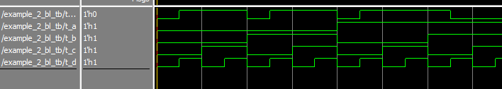
You can also verify the design by writing the output expression and verifying it using the truth table.
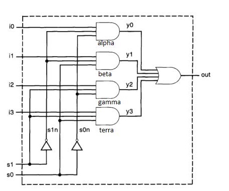
Example-3: Implement 4×2 Multiplexer using gate level Modeling as shown below:
Verilog Code:
module example_3_bl(out, i0, i1, i2, i3, s1, s0);
input i0, i1, i2, i3, s1, s0;
output out;
wire y0, y1, y2, y3, s1n, s0n;
not n1(s1n, s1);
not n2(s0n, s0);
and alpha(y0, i0, s1n, s0n);
and beta(y1, i1, s1n, s0);
and gamma(y2, i2, s1, s0n);
and terra(y3, i3, s1, s0);
or out2(out, y0, y1, y2, y3);
endmodule
Test Bench Code:
module example_3_bl_tb;
wire t_out;
reg t_i0, t_i1, t_i2, t_i3, t_s1, t_s0;
example_3_bl my_mux(.i0(t_i0), .i1(t_i1), .i2(t_i2), .i3(t_i3), .s1(t_s1), .s0(t_s0), .out(t_out));
initial
begin
// 1
t_i0 = 1'b0;
t_i1 = 1'b0;
t_i2 = 1'b0;
t_i3 = 1'b0;
t_s1 = 1'b0;
t_s0 = 1'b0;
#5 //2
t_i0 = 1'b0;
t_i1 = 1'b0;
t_i2 = 1'b1;
t_i3 = 1'b1;
t_s1 = 1'b0;
t_s0 = 1'b1;
#5 //3
t_i0 = 1'b0;
t_i1 = 1'b1;
t_i2 = 1'b1;
t_i3 = 1'b0;
t_s1 = 1'b1;
t_s0 = 1'b0;
#5 //4
t_i0 = 1'b1;
t_i1 = 1'b0;
t_i2 = 1'b1;
t_i3 = 1'b1;
t_s1 = 1'b1;
t_s0 = 1'b1;
#5 //5
t_i0 = 1'b1;
t_i1 = 1'b0;
t_i2 = 1'b0;
t_i3 = 1'b0;
t_s1 = 1'b1;
t_s0 = 1'b1;
end
endmodule
Simulated Results for selected test inputs is shown below:
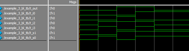
The above result shows the simulated results for selective inputs as given in test bench code. As we can see in the above result when switches (s0 = 0) and (s1=1) the output should be i3 which it is. You can try implementing the above code in Modelsim and try with your own set of inputs.
These three examples will help you clear out the idea of gate level modelling using Verilog. If you have any confusion or questions please write in a comment section.