In the Previous article How to Simulate in Xilinx Project Navigator using Verilog, we have explained step-by-step instructions on how we can simulate Verilog programs using Xilinx ISE Project Navigator. This article will be a continuation of that article and in this, we will program our FPGA. For this to work you need the following items:
Things you need:
- Xilinx FPGA Board (we will be using Spartan-6 XC6SLX9) Buy here
- Xilinx Platform USB cable. (you can use j-tag cable if you have an old PC having LPT port) Buy here
- Xilinx ISE (Project Navigator & iMPACT)
- Verilog coding skills
Cheapest FPGA to buy for beginners:
You can use any compatible Xilinx board and if you have a Digilent series board like Basys 3 you don’t need platform cable as these board contains Atmel chips on them and can be programmed directly with USB cable using Adapt (no need for platform cable hardware). If you are new to FPGA programming I will encourage you to buy Digilent series training board like Basys 3 or similar as they are specially designed for students and learners. Though they are expensive starting $100 and above, whereas Spartan-6 board from AliExpress and platform cable combined costs around $50. Remember, platform cable from AliExpress or similar is Chinese made whereas original costs around $200 (Buy original Xilinx USB platform cable).
Platform cable has an upper edge as it can be used to program all Xilinx devices using J-TAG. Whereas, Digilent board don’t have this flexibility. Though, Digilent has introduced another product JTAG-HS3 Programming cable which can be used to program Xilinx devices.
Conclusion: So, if you have a budget of around $100 or more I recommend a Basys 3 board as they contain internal programming circuitry so you don’t need a separate programming cable. But if you have a limited budget and want more flexibility I will recommend Xilinx USB platform cable with any cheap board like X-SP6-X9.
Programming stages for both boards are same except for the burning part.
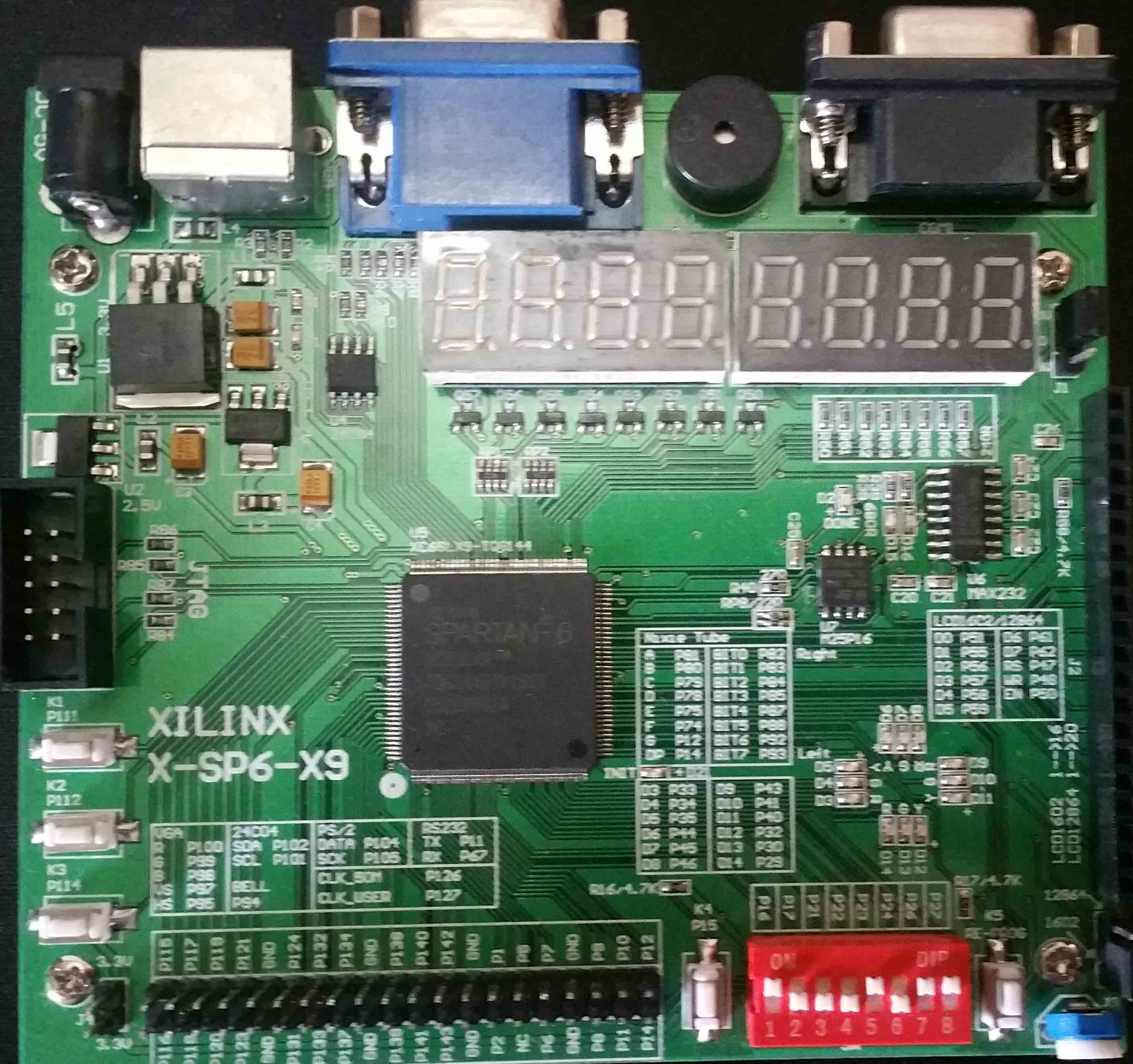
Above board, X-SP6-X9 contains Xilinx FPGA chip XC6SLSX9 of Spartan-6 series. This board is custom made board contains many I/O like 7-segment displays, LED lights, DIP switches, LCD interface option, push button switches, serial port interface, VGA display etc. This board is cheap costs around $24 and perfect for learning.
Datasheet: More details of FPGA chip XC6SLX9 can be found here
We will use platform cable to burn basic LED on/off code on the above board.
Stages of Programming:
- Design your circuit (LED on/off using push button)
- Define Inputs and Outputs
- Write Verilog code (verify it using Project Navigator explained here)
- Mapping of inputs and outputs to hardware (using PlanAhead)
- Synthesis your code
- Implement Design (Translate, Map, Place & Route)
- Generate Programming File (.bit file)
- Configure Target Device (can be Digilent board or the X-SP6-X9)
We will follow the above stages throughout this tutorial. Before beginning, I hope you are familiar with Verilog simulation using Xilinx Project Navigator and some basic concepts of Verilog.
Stage-1,2,3: Design your Circuit
Since we are just testing our FPGA board we will write a basic program on our FPGA like LED on/off using push button.
Follow the instructions given in Verilog Simulation and FPGA setup using Xilinx Project Navigator on project settings and device parameters. You may leave input/output ports for now and write the following code:
Verilog Code:
module led_on_off(
input a,clk,
output reg b
);

always @(posedge clk)
 b <= a;

endmodule
Verify the above code using Behavioral Check Syntax on lSim simulator.
Stage-2: Mapping of Inputs & Outputs to Hardware
Now you have written your Verilog code and tested it on simulation. The next step is to move that code on FPGA board. But, wait. How does your board know which LED to turn ON on pressing button ?. The answer lies in the mapping of inputs and outputs. This can be achieved using PlanAhead.
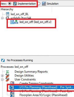
PlanAhead comes with Xilinx ISE. Change view to Implementation and double click on I/O Pin Planning (PlanAhead) Pre-Synthesis under User Constraints as shown above.
Upon double clicking, PlanAhead will open, if any dialog box appears asking that a new user constraint file will be added to project select Yes.

Hold board in your hand and make a choice that which LED you wants to turn ON/OFF. This board contains 12 LED’s so let’s say we select D5. A small table is also printed with these LED lights which tell us that D5 is connected to P35 of FPGA i.e. D5 is connected to port 35 of FPGA. This board contains 5 push button switches. I will pick K4 which is connected to P15 of FPGA as shown in the right picture.
Many FPGA board comes with 50Mhz, 100Mhz, 25Mhz clocks. You can custom define your clock. Alternatively, you can use programming practices to change your clock speed. clocks are connected to specific ports on FPGA and are mentioned with port numbers on a board. For our case, we will be using a clock of 50Mhz which is connected to P126 (It is highlighted on board). Also, make sure you select I/O standard as LVCMOS25. Configured PlanAhead will look like:
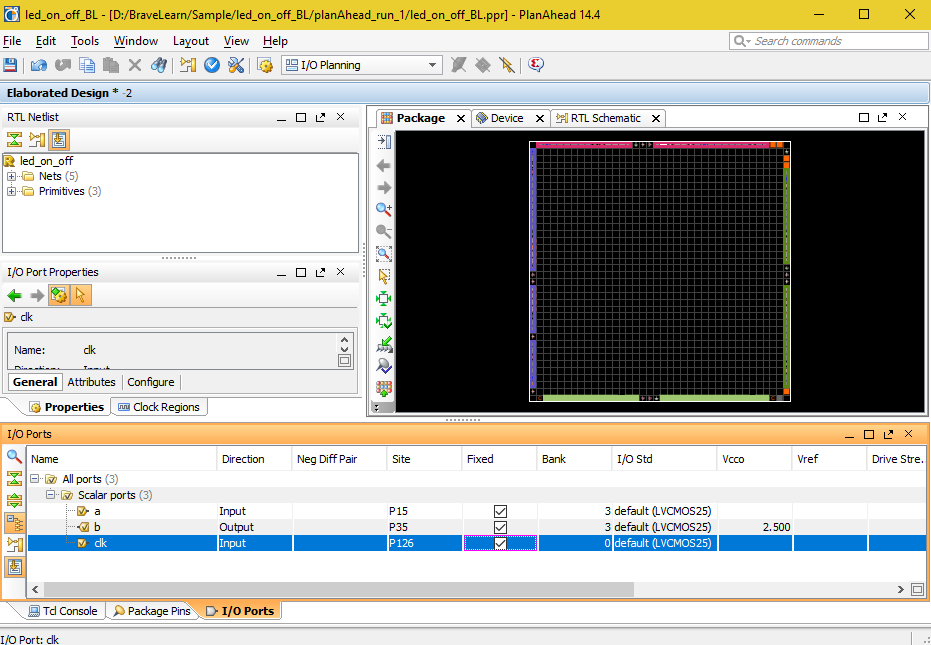
Save the settings by using Ctrl+S and close the PlanAhead. A new led_on_off.ucf file will be created in your project.
Stage 5,6,7: Synthesize, Implement Design, Generate Programming File.
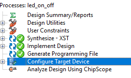
If you have completed the above stages carefully, then double click on Synthesize. A process circle will start and after successful synthesis, a green check mark will appear. Similarly, double click on Implement Design and then double click on Generate Programming File.
If a green checkmark appears with Generate Programming File as shown, then Congratulations! you have successfully generated a .bit file which contains binary instructions to turn LED ON or pressing push button.
Stage-8: Configure a Target Device
In this last stage, we will burn our design on FPGA board. If you have Xilinx USB platform cable then double click on Configure Target Device and if you have Digilent Basys-3 board use the .bit programming file and Adapt to burn the code on your Digilent board.
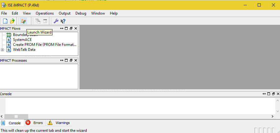
iMPACT will open after clicking configure Target Device. Make sure you have connected Xilinx USB cable and your FPGA board is powered ON. Click Launch Wizard in iMPACT
A dialog box will appear. Select Configure device using Boundary Scan (J-TAG) and select Automatically connect to a cable and identify Boundary-Scan chain and click OK. iMPACT will automatically detect your FPGA board and will ask you to select .bit file.
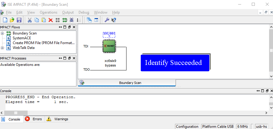
Right click on Xilinx green chip in iMPACT and select “Assign new configuration file”. Locate the .bit file we have generated previously.
If iMPACT asks to attach SPI/BP PROM file select NO. Attaching SPI/PROM files make sure that upon power failure your program is not lost.
Right click on green chip again and select Program.
Note: This board is active Low, means all unused pins are active as Xilinx pulls-down by default. If you are using this board you may see all LED lights are turned ON, the buzzer is making sound etc. To overcome this problem right click on Generate Programming File and select Properties->Configuration Options -> Change unused pins from pull-down to pull-up.
Congratulations! you have successfully burned a program on your FPGA board. If you have any suggestions or questions please leave us a comment below:
