In this tutorial, we will show you how you can interface seven-segment display with FPGA board and display a number on it.
Before continuing, make sure you understand the basics of FPGA programming (Verilog), know how one uses Xilinx Project Navigator to simulate Verilog programs and How one can program a code on FPGA board.
Things you need:
- FPGA board (we will be using Xilinx X-SP6-X9) / FPGA chip with J-TAG / Any Digilent board
- Xilinx ISE (Project Navigator, PlanAhead, iMPACT)
- Seven-segment display (many development boards contains on board seven-segment display)
- Xilinx platform cable (in case of Xilinx FPGA) / (no need if you are using Digilent boards)
- connecting wires (if your board don’t have a seven-segment display)
Seven-Segment Display:

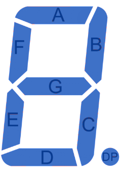
A seven segment display as shown on the right contains seven illuminating lights known as segments and the 8th dot point light. All of these seven LED’s are connected with common anode or cathode depending on the type you buy. A seven-segment display is used to display information in hexadecimal (0-F). Since seven segment display contains LED’s as their source of illumination and LED is nothing but a diode having cathode and anode. All of these segments are joined together to form two variants which are available in the market:
- Common Cathode Display: In common cathode display, cathodes of all segments are joined together to form one wire which is connected to ground or LOW logic. Individual segments are turned ON by connecting their anodes to HIGH logic. A pin configuration is shown below:

- Common Anode Display: In this other type, all segments have their anode joined together which are connected to HIGH logic and individual segments can be turned ON by connecting to LOW logic.

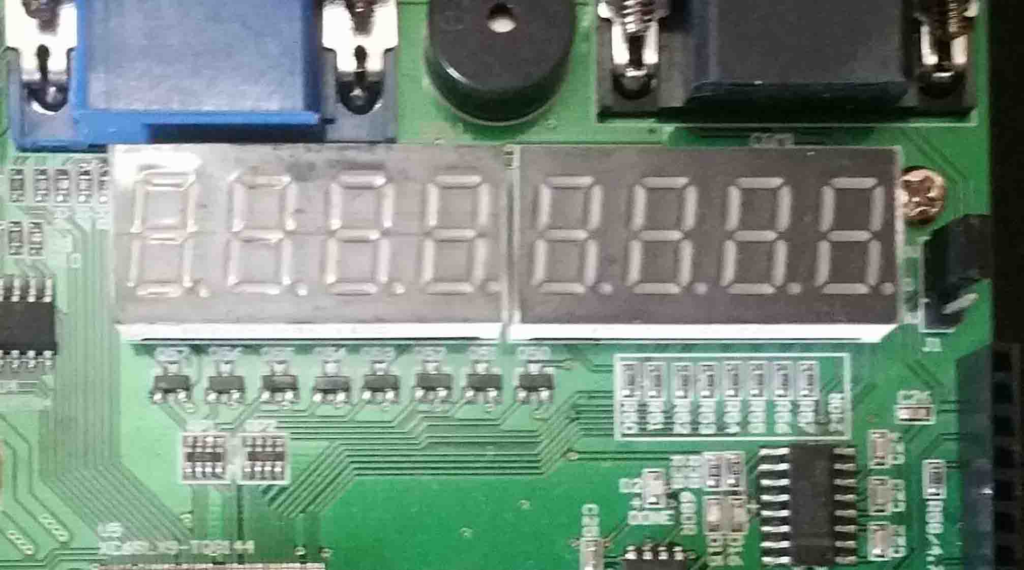
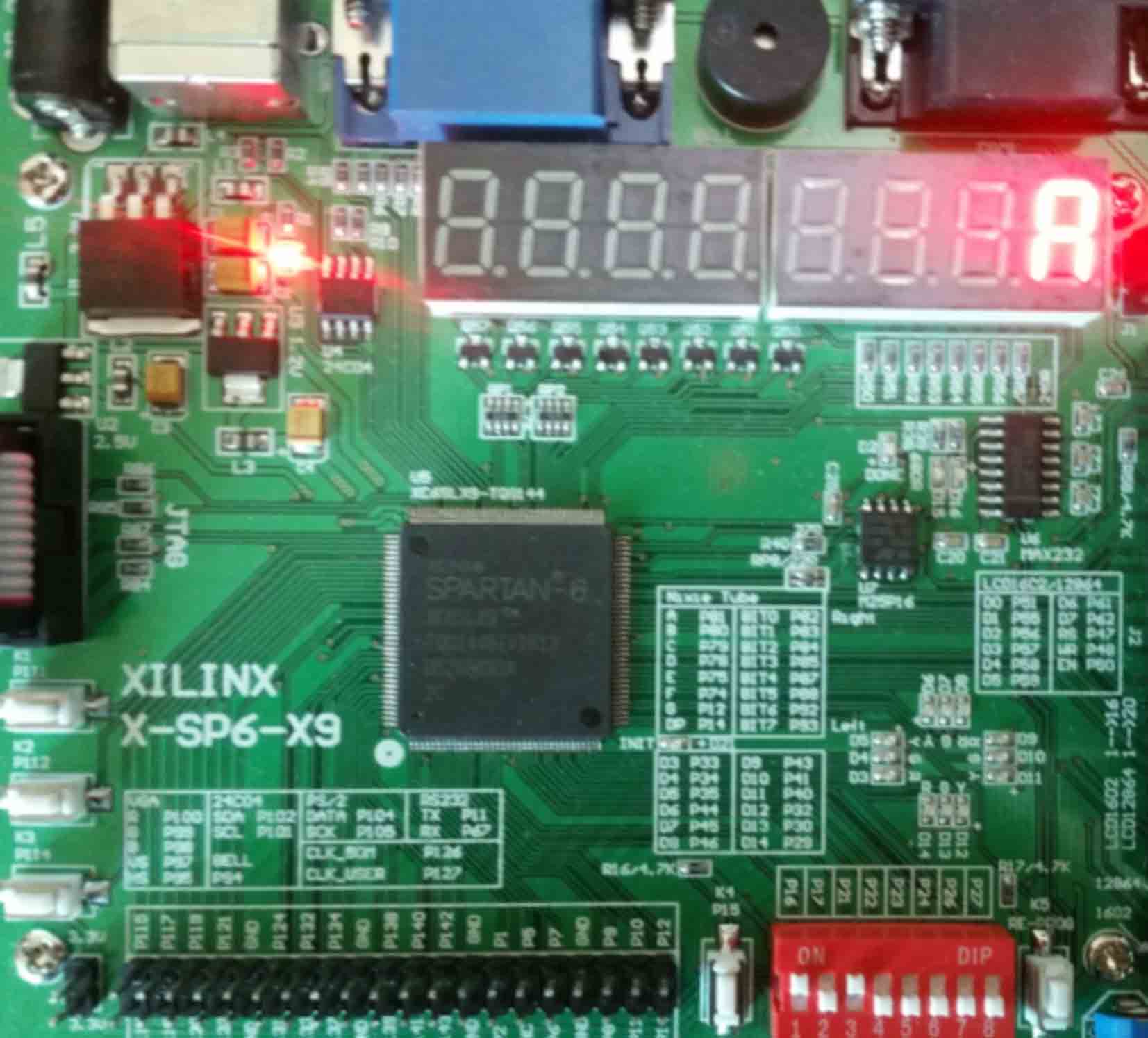
Interfacing with FPGA: The board we are using in this tutorial is Xilinx X-SP6-X9 which contains on board 8 seven-segment displays as shown.
This board contains 4 seven-segment displays in 2 packages. For each package contains 4 seven segment displays having 4 common anode points and 8 segments including dot point. To display a 4-digit number is a challenging as it requires all 4 displays to turn on simultaneously with all displaying different number. This task will require the use of on board clock. We are skipping this task for our next tutorial and will be using a single seven-segment display to display our number.
Problem: Display hexadecimal number on seven-segment display as output and use on board dip switches as BCD input of a number using FPGA board.
If you don’t have dip-switches on your board and no means of entering input then you can simply make a small change in Verilog code to display any number from 0-F.
In traditional circuit designing where we don’t use FPGA, one could use a BCD to the seven-segment decoder to translate a 4 input number to a seven display number. For this purpose, there are ready-made decoders like TTL 74LS47 available in the market.
We will be using hierarchical style coding of Verilog in which we will employ two blocks:
- Decoder block (converting a BCD number to seven-output number)
- Main block (takes input from dip switches and pass the number to decoder)
A decoder here will act as a multiplexer which takes 4-bit BCD input and outputs a 7-bit number. Dot point will be LOW all the time. A block diagram is shown below:

Verilog Code: A Verilog code for both blocks is given below:
Decoder Block:
module BCD_to_seven_segment(ca,cb,cc,cd,ce,cf,cg,disp_num);

output ca,cb,cc,cd,ce,cf,cg;

input [3:0] disp_num;
wire [3:0] mux_select;

assign mux_select = ~disp_num;

assign {ca,cb,cc,cd,ce,cf,cg} = (mux_select == 0) ? 7'b0000001 : (mux_select ==  1) ? 7'b1001111 : (mux_select == 2) ? 7'b0010010 : (mux_select == 3) ? 7'b0000110 : (mux_select == 4) ? 7'b1001100 : (mux_select == 5) ? 7'b0100100 : (mux_select == 6) ? 7'b0100000 : (mux_select == 7) ? 7'b0001111 : (mux_select == 8) ? 7'b0000000 : (mux_select == 9) ? 7'b0000100 : (mux_select == 10) ? 7'b0001000 : (mux_select == 11) ? 7'b1100000 : (mux_select == 12) ? 7'b0110001 : (mux_select == 13) ? 7'b1000010 : (mux_select == 14) ? 7'b0110000 : 7'b0111000;

endmodule
The above code uses Data-flow modeling of Verilog and employs a simple multiplexer which selects the output for a given number. Since we are using only one seven-segment display we will select which one in our main code by turning its anode to LOW.
You may note an anomaly in the above code as we have inverted our BCD input, this is optional for easy selection of input as the board we are using is active LOW. You can remove the inversion if you want.
Main block:
module display_number_BL(dip_switch,an0,ca,cb,cc,cd,ce,cf,cg);

input [3:0] dip_switch;
output an0,ca,cb,cc,cd,ce,cf,cg;

assign an0 = 0;

BCD_to_seven_segment drive_1(ca,cb,cc,cd,ce,cf,cg,dip_switch);

endmodule
In above code, we have selected left most seven-segment as our choice of display. You can use different seven segment display if you want. If you are using separate seven-segment display then make sure you turn its common anode/cathode to proper logic.
Follow the steps indicated in How to burn code on FPGA board. A brief summary of steps is given below:
- Compile the above code and check for syntax errors which there shouldn’t be any using Behavioral Check Syntax.
- Synthesize the code.
- One more thing you might want to do is to connect your ports in Xilinx ISE using PlanAhead. An “ucf” (user-constrained file) will be created and added to your project as explained here. If you are using the same board X-SP6-X9 then an “ucf” file code is given below:
# PlanAhead Generated physical constraints NET "dip_switch[0]" LOC = P22; NET "dip_switch[1]" LOC = P21; NET "dip_switch[2]" LOC = P17; NET "dip_switch[3]" LOC = P16; NET "an0" LOC = P82; NET "ca" LOC = P81; NET "cb" LOC = P80; NET "cc" LOC = P79; NET "cd" LOC = P78; NET "ce" LOC = P75; NET "cf" LOC = P74; NET "cg" LOC = P12; - Implement Design
- Generate Programming File (If you have an active LOW board like X-SP6-X9 then make sure to change properties of Generate Programming File and select all unused pins to “Pull up“.
- Use Xilinx platform cable and iMPACT to transfer your bitstream on your FPGA board. Or if you have Digilent board use Adapt to transfer your code.
After performing above steps, you have successfully displayed a number on a seven-segment display using dip-switches as input.

If you have any questions or suggestions please leave us a comment below:

Hello, could you tell me what kind of JTAG cable and JTAG programmer you are using to program this board? Thanks a lot!
You can use the official Xilinx platform USB JTAG cable or buy a third-party version from Aliexpress. The platform cable comes with connecting cable that connects to this board.